
Mon - Sat 9:00 - 17:30
In the past one year, all of us must have heard that India is ambitiously working towards becoming a leader in manufacturing semiconductors. But before we dive into fire safety, let’s pause—do you know what semiconductors actually are, where they are used, and why they are so important?
Semiconductors are the backbone of modern electronics. They are tiny chips that control and power everything from smartphones, computers, cars, medical devices, satellites, and even defense systems. The global demand for these chips is skyrocketing, and India’s push to establish a strong semiconductor manufacturing base is a step towards self-reliance and technological leadership.
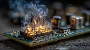
But here comes the critical aspect—manufacturing semiconductors is not only highly complex but also hazardous from a fire safety perspective. Understanding these hazards is essential for both industry professionals and emergency responders.
Wafer Preparation → Photolithography → Etching → Deposition → Doping/Ion Implantation
       ↓
  Metallization (Reactive Metals) → Cleaning & CMP → Testing & Packaging
The production of a semiconductor chip happens in ultra-clean environments called fabs. The process has several stages, and many of them involve flammable, toxic, or reactive materials.
Silicon ingots are sliced into wafers and polished.
Fire Hazard: Minimal, mostly dust/electrical hazards at this stage.
A light-sensitive chemical called photoresist is applied on wafers. Ultraviolet light is used to print circuit patterns.
Fire Hazard: Solvents like isopropyl alcohol (IPA), acetone, and other organics are highly flammable.
Unwanted material is removed using plasma etching or wet chemicals.
Fire Hazard: Use of toxic gases like chlorine, fluorine, and corrosive acids. Some gases (e.g., silane, phosphine) are pyrophoric, igniting spontaneously in air.
Thin films of materials are deposited on the wafer using gases.
Fire Hazard: Flammable gases such as hydrogen, silane, dichlorosilane are common. These can cause explosions if leaked.
Introducing impurities into silicon to alter conductivity.
Fire Hazard: Gases like arsine, phosphine, diborane are not only toxic but also highly reactive.
Conductive paths are formed by depositing metals like aluminum, copper, titanium, tungsten, or magnesium.
Fire Hazard: Metals like aluminum and magnesium are reactive; if ignited, they burn at very high temperatures and cannot be extinguished by water or foam.
Special Risk: Metal fires generate their own oxygen, making traditional extinguishing agents ineffective.
Slurries, acids, and solvents are used to clean and smooth the wafer.
Fire Hazard: Flammable solvents (IPA, ethanol), corrosive acids, and risk of toxic vapor release.
Chips are cut, wired, and sealed into packages.
Fire Hazard: Mainly electrical and minor solvent hazards.
👉 In summary: Deposition, Etching, Doping, and Metallization are the highest fire risk stages.
When a fire breaks out in a semiconductor facility, firefighters and emergency responders face unique challenges:
Toxic Fumes: Burning chemicals may release deadly gases like hydrogen fluoride (HF), arsine, and phosphine.
Explosion Risk: Gas cylinders and chemical tanks may explode under heat.
Confined Spaces: Fabs have complex layouts with narrow corridors and cleanroom suits, making evacuation and firefighting difficult.
Contamination Risk: Water, foam, or chemical runoff can damage sensitive equipment and contaminate cleanrooms.
Reactive Metal Fires: Aluminum or magnesium fires cannot be fought with water or CO₂.
Should Use:
Inert Gas Suppression Systems (CO₂, Nitrogen, Argon blends): Effective for controlling gas and electrical fires (not for reactive metals).
Dry Powder (Class D agents such as graphite, sodium chloride, or copper powder): For reactive metal fires like aluminum or magnesium.
Specialized Clean Agents (FM-200, Novec 1230): Protect cleanroom equipment without contamination.
Water Spray (in controlled applications): For cooling tanks and preventing explosions, but not directly on burning chemicals or reactive metals.
Should Avoid:
Foam:
Not suitable in cleanrooms because it introduces moisture and particulates that destroy the controlled environment, contaminate wafers, and permanently damage sensitive electronics.
Incompatible with certain chemicals:
Reactive metals (Aluminum, Magnesium, Titanium): Foam contains water; it reacts violently with burning metals, releasing hydrogen gas and potentially causing explosions.
Strong oxidizers (e.g., nitric acid, perchlorates): Foam can break down or intensify the reaction, worsening the fire.
Hydrofluoric acid residues: Water-based foam may release highly toxic hydrogen fluoride gas upon contact.
Plain Water Jet: Spreads flammable liquids and reacts dangerously with burning metals.
CO₂ on Metal Fires: Ineffective and may cause splattering of molten metal.
A well-structured firefighting strategy should be in place, which includes:
Prevention First
Gas detection and leak monitoring systems.
Automatic suppression systems integrated with process tools.
Proper ventilation and exhaust systems.
Response Plan
Evacuate personnel immediately due to toxic gas risk.
Isolate chemical supplies using emergency shutoff valves.
Use specialized agents based on the fire class.
Responder Protection
Full protective gear with SCBA (Self-Contained Breathing Apparatus).
Training in hazardous materials (HAZMAT) response.
Awareness of fab layout and chemical storage locations.
Post-Fire Considerations
Decontamination of equipment and areas.
Monitoring for toxic residues and airborne chemicals.
Controlled disposal of contaminated firefighting runoff.
As India takes bold steps towards becoming a global hub for semiconductor manufacturing, fire safety must stand as a parallel priority. These facilities are not just high-tech but also high-risk. Emergency responders need specialized training, protective equipment, and awareness of the unique hazards involved—especially when reactive metals and toxic gases are present.
By adopting prevention, rapid detection, and tailored firefighting strategies, we can ensure that India’s semiconductor dream is built on a foundation of both innovation and safety.
We offer a full suite of HSEFS services designed to address your specific challenges and goals :
HSE Consulting & Advisory,
HSE Auditing & Assurance,
HSE Training & Development,
Implementation & Support,
Environmental Services
GST: 24ABDCA0826H1Z3
CIN: U71100GJ2025PTC163795
Copyright 2025. Agni Raksha Niti Engineering Consultancy Services Pvt. Ltd. All Rights Reserved.